
The AXI Protocol
The Advanced eXtensible Interface, commonly known as AXI, is an on-chip communication bus protocol developed by ARM (Advanced RISC Machine) as part of their AMBA (Advanced Microcontroller Bus Architecture) specification back in 2003. It was later defined as AXI4 in a revision of the AMBA4 protocol in 2010. The AXI protocol's core highlight is the framework for determining how different blocks within each chip communicate with each other. It provides a methodology before any data is transmitted to demonstrate presence and uninterrupted information exchange, enabling different systems to communicate without stepping on each other.
The Memory Controller
One of the interconnected systems can be a memory present in the system. A memory controller, therefore, is needed to communicate between the two. The memory controller would consist of an interconnect to connect multiple AXI interfaces, which we will call masters to multiple slaves, with one of the slaves being the memory block. When data transfer takes place, the interconnect establishes a connection between the masters and the slaves. The AXI Memory Controller connects to the AXI protocol through the AXI interface on one side. On the other side, it connects to the SRAM through basic protocol. The memory controller breaks down the AXI interface signals and passes necessary information to SRAM to write or fetch data from specified address locations.

Handshake
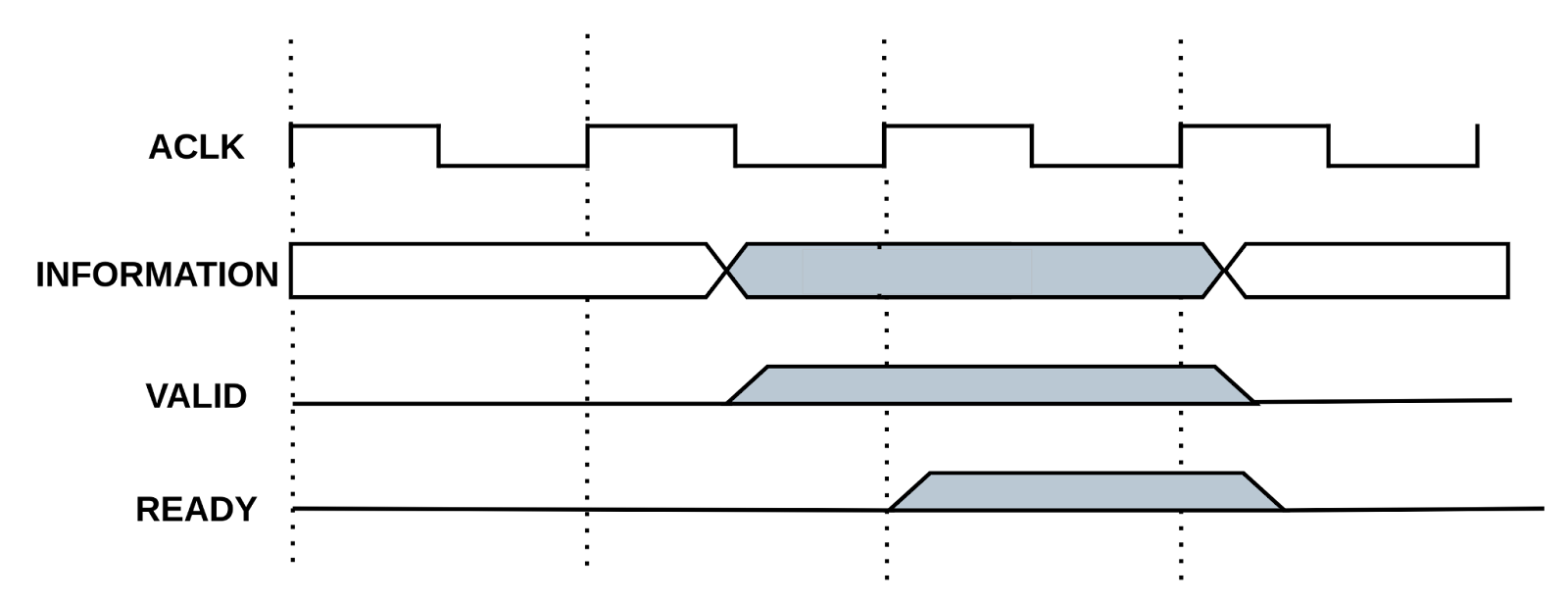
The handshake protocol is a must before any data transfer. Idea is as simple and intuitive as a real-life handshake. A person raises their hand upon meeting another person to assert that they are ready to communicate with them. The other person acknowledges it and shakes the hand. This gesture establishes a connection between them and a conversation or “data transfer” may then take place. The AXI4 provides a similar protocol to initiate data communication. When address, data, or control information is accessible, the source generates a VALID signal. A READY signal is generated by the receiver to indicate it’s readiness to receive data. When both the VALID and READY signals are HIGH, the transfer takes place.
The memory controller was designed in SystemVerilog. The architecture's five channels are described as follows:
- Read Address channel (AR)
- Read Data channel (R)
- Write Address channel (AW)
- Write Data channel (W)
- Write Response channel (B)
AXI Transaction Channels and Handshake pair.
Transaction Channel:
- WRITE ADDRESS CHANNEL
- WRITE DATA CHANNEL
- WRITE RESPONSE CHANNEL
- READ ADDRESS CHANNEL
- READ DATA CHANNEL
Handshake pair:
- AWVALID, AWREADY
- WVALID, WREADY
- BVALID, BREADY
- ARVALID, ARREADY
- RVALID, RREADY
The Design and Verification
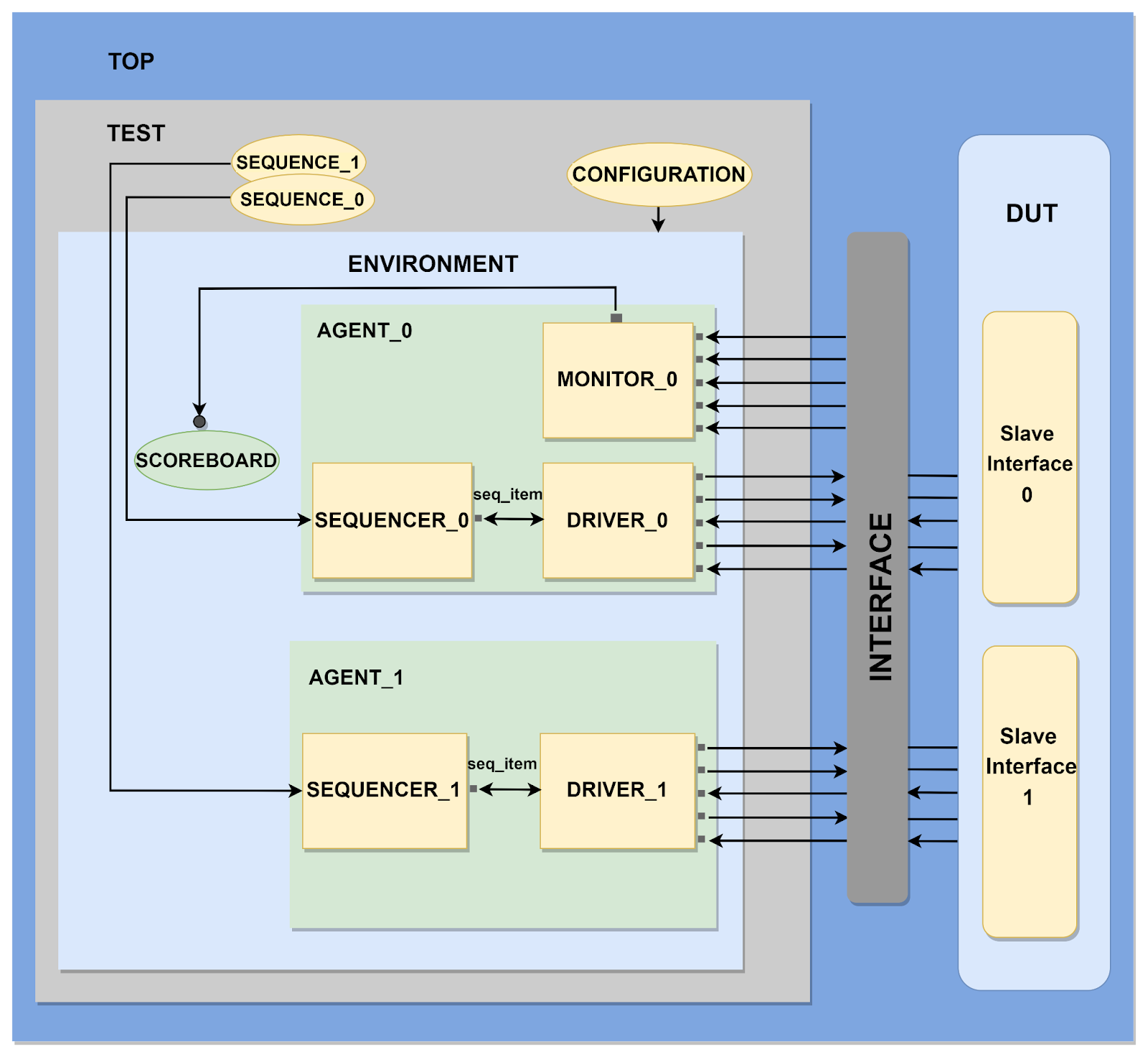
The design of this memory controller was done using SystemVerilog. Verification was done using the Universal Verification Methodology, popularly known as UVM. Maintaining a proper structure is important in projects of such scale. UVM helped with its inherited class properties for thorough verification of the designed project. An out-and-out test plan was devised to ensure proper coverage. Drivers, monitors, stimulus generators, and scoreboards are all essential components of any verification testbench. UVM provides a base class for each of these components - complete with standardized functions for instantiating, connecting, and constructing the testbench environment. In a verification environment, these are static entities called components that exist throughout a simulation, much like buildings in a city. These components operate and process data that flows around the environment in the same way that people and vehicles do in a city. Because the data or transactions appear and disappear at different times in the simulation and are dynamic in nature, they are referred to as objects or sequence items. The following shows a figure of the UVM structure used in the project.
Overall, the project consisted of a complete design and verification of an AXI memory controller made from scratch. The experience gained from this project remains indispensable to the team, helping the team gather crucial insights on industry-standard protocols and verification standards.