
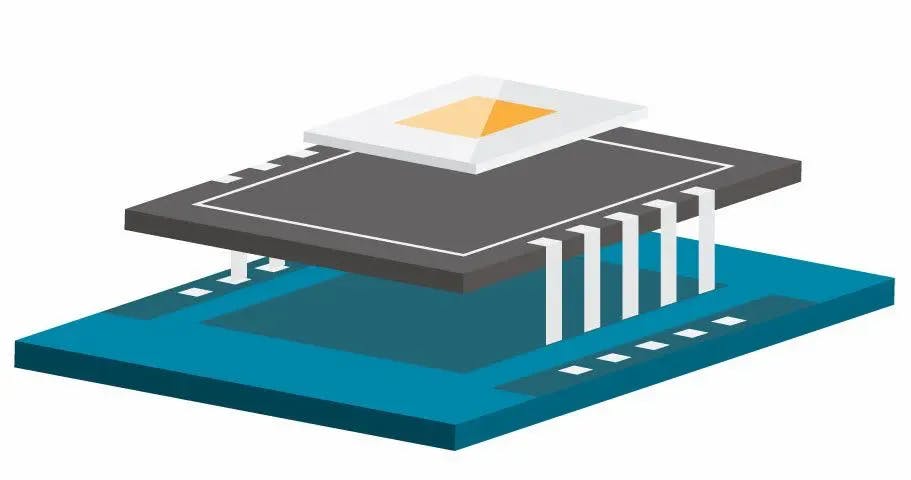
Your complete RTL-to-GDSII solution, delivering efficiency and expertise at every step of the process. Trust us to bring your semiconductor designs to life seamlessly and successfully.

 Integrate
 Turn-Key Solution
 PDK & Library Evaluation
 Synthesis
 DFT and ATPG
 Formal Verification
 Place and Route
 Physical Verification
 Timing Closure
 Power/IR Analysis
 Post-Silicon ECO
- PPA analysis for multiple frequencies, technology node, standard cell libraries to pick the most suitable node and constraints

- Physical-aware
- CPF/UPF
- 3rd Party IP integration

- ATPG and Coverage Analysis
- ATPG Simulation

- RTL to gate-level and gate-level to post-layout LEC to ensure functional integrity

- LEF/DEF Flow
- Digital Top
- Integration of Analog blocks
- EDI-OA Interoperability
- Mixed-Signal, Analog-on-top

- LVS
- DRC
- ERC
- DFM

- Parasitic Extraction
- Static Timing Analysis
- MMMC
- Timing ECO
- DSTA, DMMMC
- IR-Aware

- Balance power consumption and speed

- Smart Spare distribution in early stage to accommodate post-silicon changes in limited layers

Read what we wrote
Get front-row industry insights
The Road to RISC-V SoC Design: My Professional Evolution

A Designer’s Odyssey in RISC-V Processor Development
Chiplet Packaging: 2.5D

USA Office
8201 164th Ave NE, Suite 200
Redmond WA 98052
United States of America
+1 (404) 287-0730
Bangladesh Office
House 177, Lane 2, New DOHS
Mohakhali, Dhaka 1206
Bangladesh
+88 02222287041
+88-01730-03-74-00
European Liaison Office
32 Swansea Court
London
E16 2RT
United Kingdom
+44 7850 051037
Connect with us
Drop us a line at


USA Office
8201 164th Ave NE, Suite 200
Redmond WA 98052
United States of America
+1 (404) 287-0730
Bangladesh Office
House 177, Lane 2, New DOHS
Mohakhali, Dhaka 1206
Bangladesh
+88 02222287041
+88017300-374-00
European Liaison Office
32 Swansea Court
London
E16 2RT
United Kingdom
+44 7850 051037
Connect with us
Drop us a line at

